NETZSCH for Massachusetts Semiconductor and Advanced Materials Teams
Semiconductors, Nanoelectronics & Advanced Materials Characterization for Massachusetts Teams
Whether you are developing thin films, semiconductor packaging, electronic materials, nanomaterials, ceramics, or composites, selecting the right characterization method is essential for reliable development, process, reliability, and quality decisions.
NETZSCH Analyzing & Testing helps R&D, materials science, process development, device engineering, reliability, and quality teams evaluate thermal analysis and thermophysical measurement solutions for their material questions.
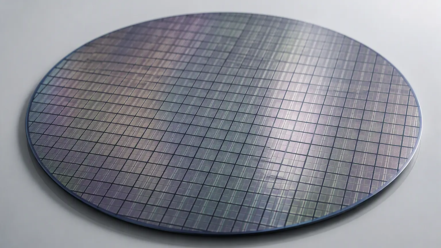
Talk to a Semiconductor Materials Characterization Specialist
Characterization Methods for Semiconductor and Advanced Materials
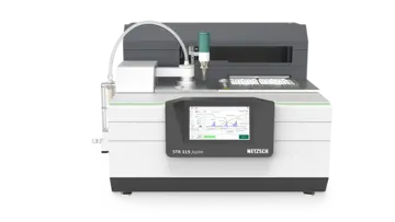
NETZSCH supports technical teams with methods for thermal, mechanical, dimensional, and thermophysical behavior - from material screening and process development to reliability and quality control.
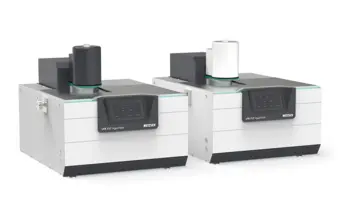
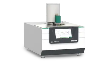
Not sure which method fits your application?
Built Around Semiconductor and Advanced Materials Requirements
For semiconductor, nanoelectronics, and advanced materials teams, instrumentation must support interconnected R&D, process development, reliability, and quality requirements. The right solution should provide method flexibility, controlled atmospheres, repeatable data quality, and meaningful correlation to thermal loads.
NETZSCH supports teams evaluating solutions for:
- Thin films, coatings, and multilayer material systems
- Semiconductor packaging and electronic assemblies
- Electronic materials, dielectrics, and encapsulants
- Nanomaterials, ceramics, and advanced composites
- Phase transitions, curing, sintering, and thermal expansion
- Thermal conductivity, volatile release, and moisture behavior
- Reliability assessment and quality control under thermal loads
From a focused material question to a repeatable characterization workflow: we help you evaluate methods that address current development targets and future reliability or quality needs.
A Technical Partner for Semiconductor and Advanced Materials Characterization
Application-focused consultation
Complementary method expertise
Support beyond instrument selection
Discuss Your Semiconductor or Advanced Materials Application
Tell us about your material, device, process, or reliability question and the property you need to understand. A NETZSCH representative will discuss suitable characterization methods and instrument options with you.
Find the Right Characterization Approach for Your Materials
You May Also Be Interested In
Explore NETZSCH Analyzing & Testing products, application insights, service offerings, and e-learning resources for thermal analysis and materials characterization.