NETZSCH for Texas semiconductor and electronics teams
Characterize Semiconductor and Electronic Materials with Confidence
For semiconductor, electronics, thin-film and functional-material development, method selection determines how reliably you can link thermal behavior to process windows, device performance and long-term reliability.
NETZSCH Analyzing & Testing helps Texas R&D, materials science, process, device, reliability and quality teams identify suitable thermal, mechanical and thermophysical characterization methods for their materials and measurement objectives.
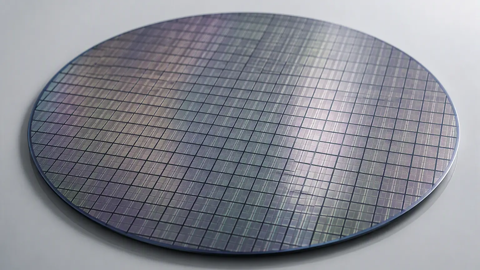
Talk to a Semiconductor Materials Characterization Expert
Characterization Methods for Semiconductor, Electronics and Functional Materials
NETZSCH supports technical teams with methods for evaluating thermal transitions, stability, mechanical response, dimensional change and heat transport across materials development, process engineering and reliability work.
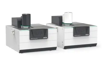
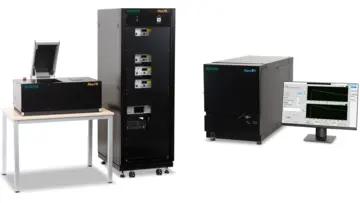
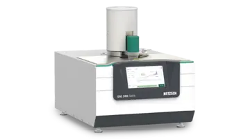
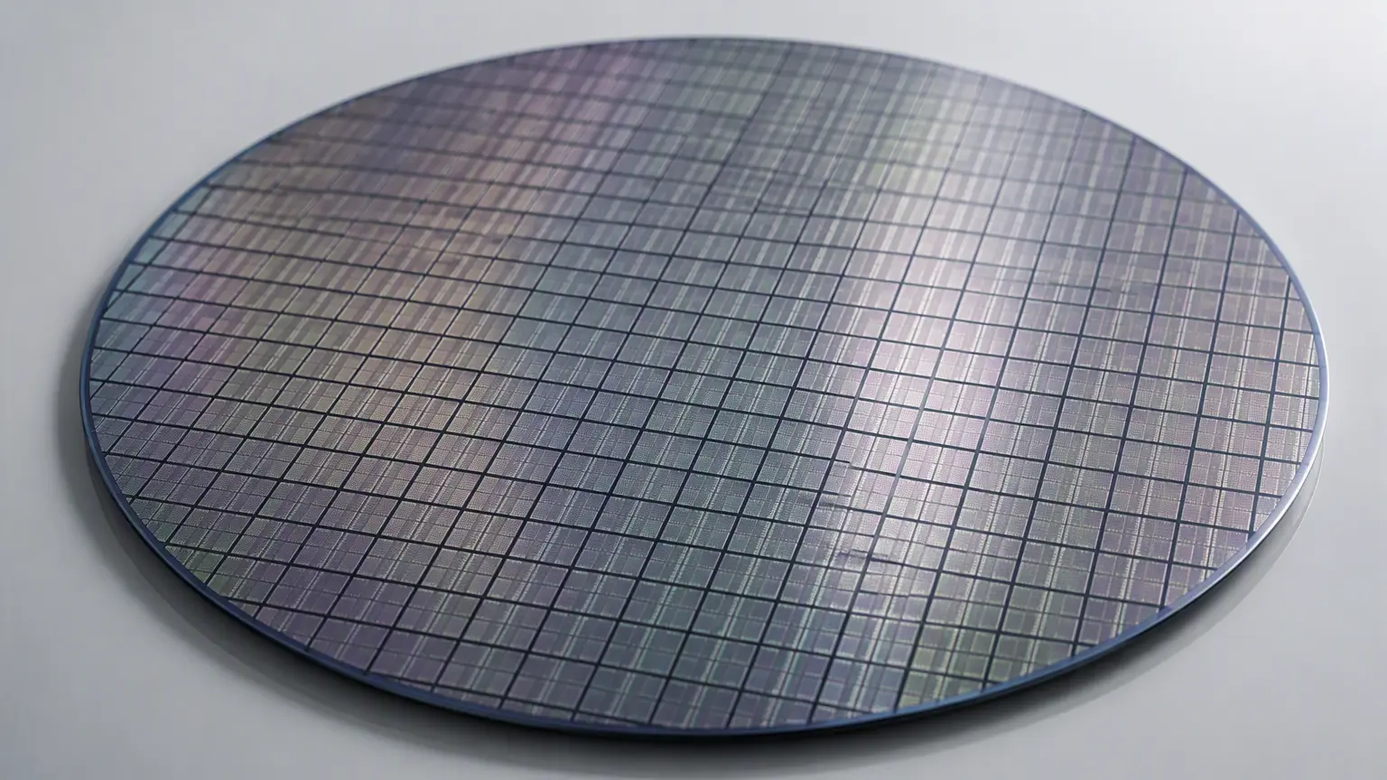
Not sure which method fits your material or device question?
Built Around Semiconductor and Electronics Development Requirements
Instrumentation decisions for semiconductor and electronic materials must support reproducible data across development, process engineering, reliability and quality workflows. The appropriate configuration depends on sample geometry, atmosphere, temperature program, throughput and the material property being evaluated.
NETZSCH helps teams evaluate methods for:
- Thin films, coatings and multilayer material systems
- Semiconductor, electronic and photovoltaic materials
- Functional ceramics, powders and nanomaterials
- Thermal transitions, phase behavior and specific heat
- OxidationOxidation can describe different processes in the context of thermal analysis.Oxidation, Thermal StabilityA material is thermally stable if it does not decompose under the influence of temperature. One way to determine the thermal stability of a substance is to use a TGA (thermogravimetric analyzer). thermal stability, Decomposition reactionA decomposition reaction is a thermally induced reaction of a chemical compound forming solid and/or gaseous products. decomposition and volatiles
- Moisture uptake, desorption and binder removal
- SinteringSintering is a production process for forming a mechanically strong body out of a ceramic or metallic powder. Sintering, shrinkage and thermal expansion
- Thermal DiffusivityThermal diffusivity (a with the unit mm2/s) is a material-specific property for characterizing unsteady heat conduction. This value describes how quickly a material reacts to a change in temperature.Thermal diffusivity, conductivity and package-interface reliability
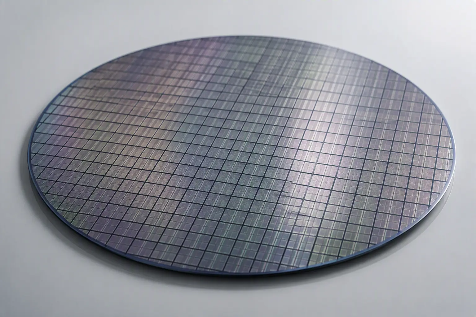
From material screening to package reliability: NETZSCH experts help Texas teams define a characterization approach that connects measurement data with process, device and quality decisions.
A Technical Partner for Semiconductor and Electronics Characterization
Application-focused consultation
Complementary method coverage
Support beyond instrument selection
Discuss Your Semiconductor or Electronics Application
Tell us about your material, sample form, development or reliability question, and the properties you need to measure. A NETZSCH expert will contact your Texas team to discuss suitable characterization methods and instrument options.
Define the Right Characterization Approach for Your Materials
You May Also Be Interested In
Explore NETZSCH products, application insights, services, e-learning and events relevant to semiconductor, electronics and functional-material characterization.